
What is the process and connection of the PCB Board?
PCB Board Processing
Process of PCB Board :
The PCB Board Processing starts with applying solder to the circuit board. The first step with the machine is to inspect the circuit board and ensure it’s aligned. Once it’s aligned, it pushes it up and then applies solder across the surface evenly and smoothly to hit all the pads. It’s now removing the excess solder leaving just the solder inside the stencil, which matches perfectly with each of the pads that parts connect the PCB. The board is lowered, and then on the inside, you can see it doing a visual inspection to ensure that they applied the solder correctly. And if it isn’t, it will reject the board, which can be washed and repeated.
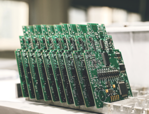
The PCB Board Processing comes out and is ready for the next stage, the pick-and-place machine. They use a manual process for low-volume prototype assembly, so they manually place the board inside. That is a two-up board meaning there are two Joule scope mainboards. The pick-and-place machine selects its tools, and then it will go and collect the individual parts and then place them on the board in rapid succession. The head moving back and forth on this pick-and-place machine can hold up to eight components simultaneously. Now the parts are coming from reels. For the most part, that is a tape and reel board, and the head travels over, picks up to eight parts at a time from the reels, and advances the reel so that the next part is ready for the next time.
They’ll speed up to eight times the speed here. The board is nearly done, and it will be working on the last few components, the larger ones. Now the last two microcontrollers are going on. And that completes the pick-and-place process. The board is now ready to be reflowed.
Connection of PCB Board :
The solder has to melt to adhere and make good mechanical and electrical connections for all the parts. It travels through this big machine and comes out the other side after it’s been PCB Board Processing. And then the solder has cooled, and all the junctions between the parts have been formed. Allied Component Works and Custom Electronics for making this possible. They’re going to take a look back. That’s the oven, the reflow oven—the pick-and-place machine. And the solder stencil machine at the very end down here.
The Joule scope beta build was a great success. After the surface mount assembly, They installed the two through-hole components. They then installed the main board inside the chassis and the front and end panels to form the complete Joule scope units. They now have several beta units that are already for early reviewers. They’ll be launching a Kick starter on February 19th, and the big challenge between now and then is growing the Joule scope community. They hop over to the Joule scope website, joulescope.com, to sign up for the newsletter. You envision a future where they change their batteries less often, where we charge our batteries less often, and in general, we have products that are just more energy efficient. Joule’s scope in the hands of makers, engineers, and developers worldwide can make this happen. If you know anyone interested in Joule scope, measuring current, power, microcontroller energy consumption.